#More than 18 Years of Experience

We offers high-quality alternative chips at lower prices, aimed at helping your Costdown.

 
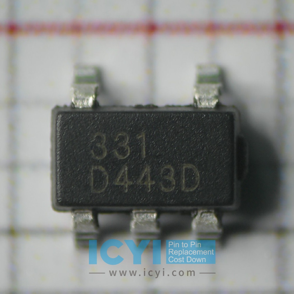
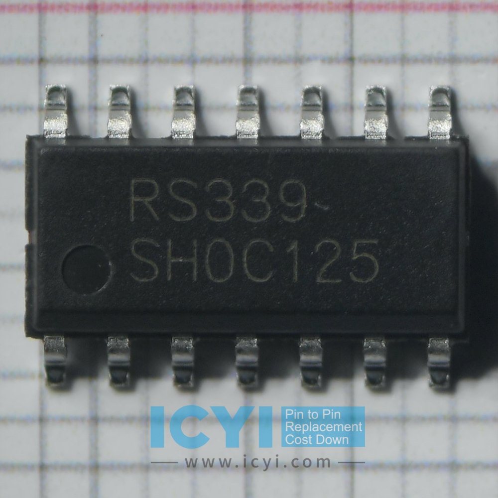
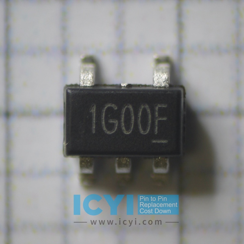
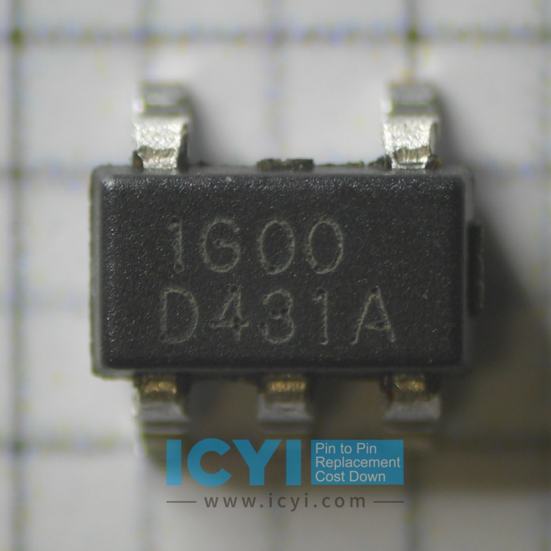
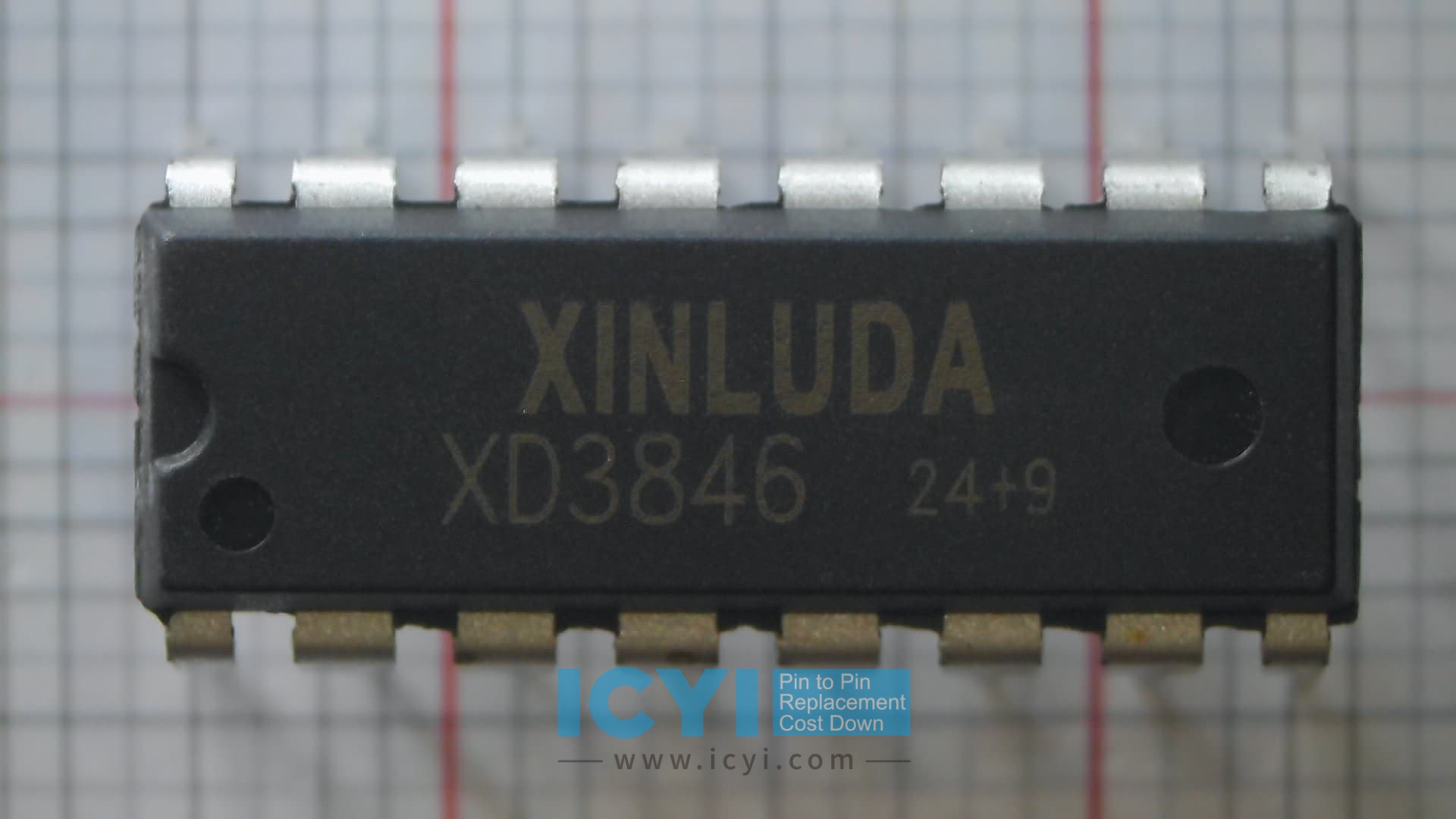
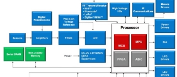
  • Diversified product lines

  • Meet various chip requirements

  • Provide free samples

Learn More
About us
More than 18 Years of Experience
Our Advantages

Why Choose Us

Your ingenuity is what turns imagination into innovation. We give you access to the components you need to breathe life into your vision.
Learn More

Latest News

April 11, 2025
How to choose parameters for operational amplifiers?
The meaning of the parameters related to operational amplifiers that will be encountered in the future will be recorded here. Recently, while using a PGA, I found that there is always a rectangular wave signal in the output when the PGA input is grounded. After amplification by 1000 times, it is very obvious, and I suspect that it is caused by interference from the power supply. At the beginning, 100uf and 0.1 capacitors were added to both the positive and negative power inputs, but the effect was not significant. Later, we planned to connect a resistor in series with the power input terminal. Initially, we chose 1k resistor, but after powering on, we found that the chip could not work at all. We measured the power supply voltage at both ends of the chip and found that it was only slightly above volts. At this point, I looked at the static current in the data manual and found that it was actually 5mA. The PGA is powered by 5V, and if the PGA works normally, the voltage division on the 1k resistor can reach 5V. So later, a 50 ohm resistor was used in combination with 100uf and 0.1uf to form a low-pass filter. This way, the chip worked normally and the output ripple was also much smaller. When choosing an operational amplifier, one should know their design requirements and search for them in the operational amplifier parameter table. Generally speaking, the issues that need to be considered in design include 1 Selection of power supply voltage and mode for operational amplifiers; 2. Selection of operational amplifier packaging; 3. Operational amplifier feedback method, which is VFA (voltage feedback operational amplifier) or CFA (current feedback operational amplifier); 4. Operational amplifier bandwidth; 5. Selection of bias voltage and bias current; 6 temperature drift; 7. Pendulum rate; 8. Selection of input impedance for operational amplifiers; 9. Selection of output driving capability for operational amplifiers; 10. Static power consumption of operational amplifiers, i.e. selection of ICC current size; 11. Selection of operational amplifier noise; 12. Operational amplifier drives load stabilization time, etc. Bias voltage and input bias current In precision circuit design, bias voltage is a key factor. For parameters that are often overlooked, such as bias voltage drift and voltage noise that vary with temperature, they must also be measured. Accurate amplifiers require bias voltage drift of less than 200 μ V and input voltage noise of less than 6nV/√ Hz. The bias voltage drift with temperature variation is required to be less than 1 μ V/℃. The indicator of low bias voltage is important in high gain circuit design, as amplifying the bias voltage may cause high voltage output and occupy a large part of the output swing. The temperature sensing and tension measurement circuit is an application example using precision amplifiers. Low input bias current is sometimes necessary. The amplifier in the light receiving system must have low bias voltage and low input bias current. For example, the dark current of a photodiode is on the order of pA, so the amplifier must have a smaller input bias current. CMOS and JFET input amplifiers are currently available operational amplifiers with the minimum input bias current. Because I am currently using a photovoltaic system for data collection, I am particularly concerned with bias voltage and current during use. If there are other needs, more consideration should also be given to other parameters at this time. 1. Input Offset Voltage (VIO) The input offset voltage is defined as the compensation voltage applied between the two input terminals when the output terminal voltage of the integrated operational amplifier is zero. The input offset voltage actually reflects the symmetry of the internal circuit of the operational amplifier, and the better the symmetry, the smaller the input offset voltage. Input offset voltage is a very important indicator for operational amplifiers, especially for precision operational amplifiers or when used for DC amplification. 2. Input Offset Voltage Drift (VIO) The temperature drift (also known as temperature coefficient) of input offset voltage is defined as the ratio of the change in input offset voltage to the change in temperature within a given temperature range. This parameter is actually a supplement to the input offset voltage, which facilitates the calculation of the drift caused by temperature changes in the amplifier circuit within a given operating range. The input offset voltage temperature drift of general operational amplifiers is between ± 10~20 μ V/℃, while the input offset voltage temperature drift of precision operational amplifiers is less than ± 1 μ V/℃. 3. Input Bias Current IB In the use of operational amplifiers, there may also be an input bias current IB, which refers to the DC current at the base of the input transistor of the first stage amplifier. This current ensures that the amplifier operates within a linear range, providing a DC operating point for the amplifier. The input bias current is defined as the average bias current at the two input terminals of an operational amplifier when the output DC voltage is zero. The input bias current has a significant impact on areas that require input impedance, such as high impedance signal amplification and integration circuits. The input bias current is related to the manufacturing process, and the input bias current for bipolar process (i.e. the standard silicon process mentioned above) is between ± 10nA and 1 μ A; For input stages using field-effect transistors, the input bias current is generally less than 1nA. For bipolar operational amplifiers, the value has a high degree of variability, but is almost unaffected by temperature; For MOS type operational amplifiers, this value is the gate leakage current, which is small but greatly affected by temperature. 4. Input Offset Current Input offset current refers to the error in bias current between two differential input terminals. The input offset current is defined as the difference in bias current between the two input terminals of an operational amplifier when the output DC voltage is zero. The input offset current also reflects the symmetry of the internal circuit of the operational amplifier, and the better the symmetry, the smaller the input offset current. Input offset current is a very important indicator for operational amplifiers, especially for precision operational amplifiers or when used for DC amplification. The input offset current is approximately one percent to one tenth of the input bias current. The input offset current has a significant impact on small signal precision amplification or DC amplification, especially when larger resistors are used outside the operational amplifier (such as 10k or more). The impact of input offset current on accuracy may exceed that of input offset voltage. The smaller the input offset current, the smaller the midpoint offset during DC amplification, and the easier it is to handle. So for precision operational amplifiers, it is an extremely important indicator. 5. Input impedance (1) Differential input impedance Differential input impedance is defined as the ratio of the voltage change at the two input terminals to the corresponding current change at the input terminals when the operational amplifier operates in the linear region. Differential input impedance includes input resistance and input capacitance, and only refers to input resistance at low frequencies. (2) Common mode input impedance The common mode input impedance is defined as the ratio of the change in common mode input voltage to the corresponding change in input current when the operational amplifier operates on an input signal (i.e. the same signal is input at both input terminals of the operational amplifier). At low frequencies, it manifests as common mode resistance. 6. Voltage gain (1) Open Loop Voltage Gain In the absence of negative feedback (open-loop condition), the amplification factor of an operational amplifier is called open-loop gain, denoted as AVOL, which is written as: Large Signal Voltage Gain。 The ideal value of AVOL is infinite, generally ranging from thousands to tens of thousands of times, and its representation can be expressed in dB and V/mV. (2) Closed Loop Gain As the name suggests, it is the amplification factor of an operational amplifier with feedback. 7. Output Voltage Swing When the operational amplifier operates in the linear region, under a specified load, the maximum voltage amplitude that the operational amplifier can output when powered by the current power supply voltage. 8. Input voltage range (1) Differential input voltage range The maximum differential input voltage is defined as the maximum allowable input voltage difference between the two input terminals of the operational amplifier. When the allowed input voltage difference between the two input terminals of the operational amplifier exceeds the maximum differential mode input voltage, it may cause damage to the operational amplifier input stage. (2) Common Mode Input Voltage Range The maximum common mode input voltage is defined as the common mode input voltage when the operational amplifier operates in the linear region and its common mode rejection ratio characteristics significantly deteriorate. It is generally defined as the maximum common mode input voltage corresponding to a 6dB decrease in common mode rejection ratio. The maximum common mode input voltage limits the range of maximum common mode input voltage in the input signal, and this issue needs to be taken into account in circuit design in the presence of interference. 9. Common Mode Rejection Ratio The common mode rejection ratio is defined as the ratio of the differential mode gain to the common mode gain of an operational amplifier when it operates in the linear region. Common mode rejection ratio is an extremely important indicator that can suppress common mode interference signals. Due to the large common mode rejection ratio, the common mode rejection ratio of most operational amplifiers is generally tens of thousands of times or more, and it is not convenient to compare directly with numerical values. Therefore, decibel recording and comparison are generally used. The common mode rejection ratio of a typical operational amplifier is between 80 and 120dB. 10. Supply Voltage Rejection Ratio The power supply voltage suppression ratio is defined as the ratio of the input offset voltage of the operational amplifier to the variation of the power supply voltage when the operational amplifier operates in the linear region. The power supply voltage suppression ratio reflects the impact of power supply changes on the output of operational amplifiers. So when used for DC signal processing or small signal processing analog amplification, the power supply of the operational amplifier needs to be carefully and meticulously processed. Of course, operational amplifiers with high common mode rejection ratio can compensate for a portion of the power supply voltage rejection ratio. In addition, when using dual power supply, the power supply voltage rejection ratios of positive and negative power supplies may not be the same. 11. Static power consumption The static power of an operational amplifier at a given power supply voltage is usually in an unloaded state. Here is the concept of static current IQ, which refers to the current consumed by the operational amplifier during no-load operation. This is the minimum current consumption of the operational amplifier (excluding sleep mode) 12. Slew Rate The conversion rate of an operational amplifier is defined as the rate at which a large signal (including a step signal) is input to the input of the operational amplifier under closed-loop conditions, and the output rise rate of the operational amplifier is measured from its output. Due to the fact that the input stage of the operational amplifier is in a switching state during the conversion period, the feedback loop of the operational amplifier does not function, meaning that the conversion rate is independent of the closed-loop gain. Conversion rate is an important indicator for large signal processing. For general operational amplifiers, the conversion rate SR<=10V/μ s, while for high-speed operational amplifiers, the conversion rate SR>10V/μ s. The current high-speed operational amplifier has a maximum conversion rate SR of 6000V/μ s. This is used for selecting operational amplifiers in large signal processing. 13. Gain bandwidth (1) Gain Bandwidth Product Gain bandwidth product, GBP, The product of bandwidth and gain. (2) Unit gain bandwidth The bandwidth when the amplification factor of the operational amplifier is 1. The concepts of unit gain bandwidth and bandwidth gain product are somewhat similar, but different. It should be noted that for voltage feedback type operational amplifiers, the gain bandwidth product is a constant, but not for current type operational amplifiers, because for current type operational amplifiers, bandwidth and gain are not linearly related. 14. Output impedance The output impedance is defined as the ratio of the voltage change to the corresponding current change when a signal voltage is applied to the output terminal of an operational amplifier when it operates in the linear region. At low frequencies, it only refers to the output resistance of the operational amplifier. This parameter is tested in an open-loop state. 15. Equivalent Input Noise Voltage The equivalent input noise voltage is defined as any AC irregular interference voltage generated at the output of an operational amplifier with good shielding and no signal input. When this noise voltage is converted to the input terminal of the operational amplifier, it is called the operational amplifier input noise voltage (sometimes also expressed as noise current). For broadband noise, the effective value of input noise voltage for ordinary operational amplifiers is about 10-20 μ V.
read more
  • February 10, 2025
    HBM - Human Discharge Model
    HBM stands for Human Body Model, which is commonly known as the human discharge model in ESD electrostatic discharge. It characterizes the chip's anti-static ability, and electronic engineers know that the higher this parameter, the stronger the chip's anti-static ability. However, different chip suppliers usually select different testing standards based on their own understanding, experience, partner resources, or the applicable application scenarios of the chip. Different standards mean that there will be differences in testing methods or conditions, and it is not possible to directly compare the anti-static ability of the chip based on the HBM numbers marked in the specification sheet. At present, the commonly used testing standards for non automotive chips include ANSI/ESDA/JEDEC JS-001 and MIL-STD-883, while automotive chips will use the AEC Q100-002 standard. ANSI(American National Standards Institute), The American National Standards Institute; ESDA(Electrostatic Discharge Association), The American Electrostatic Discharge Association; JEDEC(Joint Electron Device Engineering Council), The Solid State Technology Association; MIL-STD(US Military Standard), That is, the US military emblem. Specific testing plans for HBM using these standards can be found online. Through comparison, it can be seen that the RC values selected for the three standard tests are all R=1.5k Ω C=100pF, There is no significant difference in the peak current and current waveform tested, but the number of pulses and the time interval between pulses tested are completely different It can be seen that there is a huge difference in HBM data, because the influence of packaging materials on ESD parameters is very small, and the anti-static ability of chips under the same grain size should be comparable. The MIL-STD-883 standard is more stringent than the other two standards, and the test data will be even smaller. Of course, more strictly speaking, taking samples from the same batch and using different testing standards for testing will make the data more convincing. Comparison data provided by electronic enthusiasts can also be found online. In summary, MIL-STD-883 standard is the most stringent and the HBM data tested is smaller; The HBM data tested according to ANSI/ESDA/JEDEC JS-001 standard will be relatively large. It should be emphasized here that the standards followed for ESD testing of chips are completely different from those followed for ESD testing of whole machine products, and the energy level of static electricity is even more different. Therefore, it is not possible to directly use the ESD testing equipment of the whole machine to conduct ESD testing on chip pins. In system level circuit design, especially at external interfaces, special attention should be paid to anti-static and anti surge protection. These integrated chips are relatively delicate and cannot be expected to play the role of discrete protective devices.
  • February 10, 2025
    Chip Knowledge - MSL (Moisture Sensitivity Level)
      MSL stands for Moisture Sensitivity Level, which characterizes the ability of a chip to withstand humid environments. It is an extremely important parameter that is often overlooked by electronic engineers. Usually, chips exposed in an open environment will absorb moisture, which may enter the plastic packaging of the chip through the pins. During SMT reflow soldering, the moisture expands due to the instantaneous high temperature, and there is a probability of the so-called "POPCORN" phenomenon occurring. Classification of humidity sensitivity levels According to the JEDEC J-STD-020D standard, MSL is classified into 8 levels, as follows: MSL1 Level - Unlimited workshop life up to and including 30 ° C/85% RH MSL2 level - workshop lifespan of less than or equal to 30 ° C/60% RH for one year MSL2a level - workshop lifespan less than or equal to 30 ° C/60% RH for four weeks MSL3 level - workshop life less than or equal to 30 ° C/60% RH 168 hours MSL4 level - workshop life less than or equal to 30 ° C/60% RH 72 hours MSL5 level - workshop life less than or equal to 30 ° C/60% RH 48 hours MSL Level 5a - Workshop life of less than or equal to 30 ° C/60% RH for 24 hours MSL6 level - immediate workshop life less than or equal to 30 ° C/60% RH (for level 6, components must be baked before use and must be reflow soldered within the time limit specified on the moisture sensitive label) It is particularly important to note that if the ambient temperature or air humidity exceeds the limit test conditions for the corresponding level, the chip can be exposed to an open environment for a shorter period of time than the time specified in the standard. The impact of humidity sensitivity level and protective measures Once moisture enters the interior of the chip, there is a probability that sufficient steam pressure will be generated during SMT to damage or destroy the components. Common damage situations include internal separation (delamination) of the plastic body from the chip or pin frame, damage to the bonding wire soldering, chip damage, or cracks appearing inside the chip (which cannot be observed on the chip surface). The most serious situation is chip swelling and bursting (known as the "popcorn" effect). In addition, after moisture enters the interior of the chip, it may also cause electrochemical corrosion. Water vapor may be ionized to generate hydroxide ions when powered on, and the hydroxide ions may react chemically with the bonding pad or even the metal layer inside the chip, resulting in the formation of hydrated oxides. The oxides will also absorb some of the water vapor, creating fragile parts at the interface between the packaging resin and the metal, leading to bonding failure. If there are potassium, sodium, and chloride ions in the moisture, it will greatly increase the probability of corrosion of the chip, lead frame, and PAD, leading to delamination or peeling. After stratification occurs, the difficulty of moisture invasion is greatly reduced, and the reliability of the chip will also be greatly reduced.         Considering both cost and actual production process control, most chips will be packaged with MSL3 humidity sensitive grade and vacuum sealed bags, while desiccants and humidity sensitive cards will be placed inside. After unpacking the chip, it is necessary to complete the surface mounting and testing as soon as possible, and then apply coatings such as three proof paint for moisture sensitive protection. Once the vacuum bag leaks, the moisture sensitive card changes color, or the package is left for too long after unpacking, it is necessary to perform baking actions according to standard procedures before use to ensure the safety of chip use. Runshi Technology's automotive standard products Runshi Technology's automotive products all use MSL1 grade, and some industrial grade products also use MSL1 grade to better cope with the harsh operating or production environments of different product systems. Cost and quality are like the trade-off between fish and bear's paw. The higher the humidity sensitivity level, the higher the cost of packaging materials and processes, and the more expensive the chip price. Electronic engineers need to choose an acceptable cost, that is, the quality level of the chip, based on SMT production control capabilities, the working environment of the finished product, and market positioning when selecting.

Frequently Asked Questions

Question: How do you ensure the quality of the domestic chips you distribute?
Answer: We work with chip manufacturers that have strict quality control systems in place. All chips undergo multiple rounds of testing at the manufacturing stage, including electrical performance testing, reliability testing, and environmental testing. Before delivery, we also conduct sampling inspections to ensure that the products meet our quality standards. Additionally, we offer a quality guarantee period during which we will handle any quality-related issues promptly.
Question: What does the warranty policy for your domestic chips cover?
Answer: Our domestic chips come with a standard warranty period. During this time, if the chip fails due to manufacturing defects, we will provide free repair or replacement services. The warranty does not cover damages caused by improper use, unauthorized modifications, or external factors such as electrical surges or physical damage. To initiate a warranty claim, please contact our customer service team and provide detailed information about the problem and the chip's serial number.
Question: What kind of technical support can I get from you after purchasing your chips?
Answer: Our technical support team consists of experienced engineers who are proficient in chip technology. We offer pre-sales technical consultation to help you select the most suitable chips for your applications. After-sales, we provide assistance in chip integration, debugging, and performance optimization. You can reach out to our technical support hotline or email for any technical issues, and we will respond promptly.
Question: How can I be sure that your domestic chips are compatible with the existing systems and components in my project?
Answer: Our domestic chips are designed with broad compatibility in mind. Before you make a purchase, our technical team can offer in-depth consultations. We will analyze your specific system requirements, including interface types, power consumption, and operating frequencies, and then recommend the most suitable chips. Additionally, we have a library of technical documentation and case studies that showcase successful integrations with a wide range of systems and components, which can help you assess compatibility.
Question: How can I ensure a stable supply of your domestic chips, especially during peak demand periods?
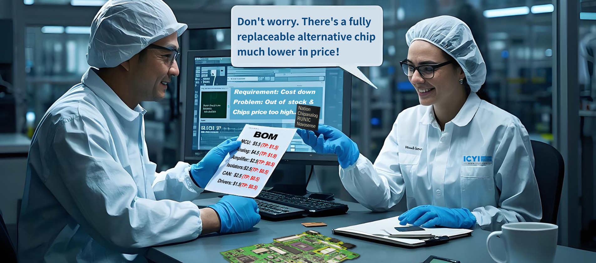
Answer: We maintain close partnerships with multiple domestic chip manufacturers. Through long-term cooperation agreements and inventory management strategies, we strive to meet the demand of our customers. We also closely monitor market trends and adjust our procurement plans in advance to ensure a stable supply. In case of unexpected situations, we will promptly communicate with you and provide alternative solutions.

Latest know-How Articles

Blog Continental Group collaborates with Novesense to create safer automotive pressure sensor chips
Continental Group collaborates with Novesense to create safer automotive pressure sensor chips   On October 24, 2024, the 2024 Continental China Experience Day, hosted by Continental Group, was held in Gaoyou City, Jiangsu Province. Nearly 200 guests from the upstream and downstream of the automotive industry chain were invited to attend the conference and engage in in-depth dialogue on the collaborative development and future trends of the automotive industry, jointly exploring future market forms and opportunities. Wang Shengyang, founder, chairman, and CEO of Novosense, and Dr. Zhao Jia, director of Novosense Sensor Product Line, were invited to attend. During the event, Novosense and Continental Group announced a strategic partnership to jointly develop automotive pressure sensor chips.   In this collaboration, both parties will focus on jointly developing automotive grade pressure sensor chips with functional safety features. The newly developed pressure sensor chip will be based on Continental's next-generation global platform, with a focus on improving reliability and accuracy. It can be used to achieve safer and more reliable systems for automotive airbags, side collision monitoring, and battery pack collision monitoring.
Blog ovosense micro car specification level 4/8-way half bridge drive NSD360x-Q1
Novosense micro car specification level 4/8-way half bridge drive NSD360x-Q1: multi load compatibility, enhancing the flexibility of automotive domain control systems     The Novosense NSD3604/8-Q1 series multi-channel half bridge gate driver chip covers 4/8 half bridge drivers and can drive at least 4 DC brushed motors, achieving multi-channel high current motor driving. It can also be used as a multi-channel high side switch driver. Very suitable for multi motor or multi load applications, such as car window lifting, electric seats, door locks, electric tailgates, and proportional valves for body control applications.     ◆ Wide operating voltage: 4.9V-37V (maximum 40V) ◆ 4, 8-channel half bridge gate drive ◆ Configurable timing charge discharge current drive (CCPD), optimized EMC performance ◆ Integrated 2-level charge pump for 100% PWM ◆ Integrated 2-channel programmable wide mode op amp  
Blog National Technology Invited to Participate in 2024 Intel
Draw a blueprint together! National Technology Invited to Participate in 2024 Intel ®  LOEM Summit November 5-7, 2024, Intel 2024 ®  The LOEM Summit was grandly held in Bangkok, Thailand, and National Technology Co., Ltd. (hereinafter referred to as "National Technology"), as Intel's global partner, was invited to participate in the summit. This summit provides an important platform for 200 Intel business partners from around the world to enhance communication and connection, share development experiences, and actively explore new opportunities in the future. Taking this opportunity, National Technology showcased its fourth generation trusted computing chip NS350, high-precision metering battery management chip NB401, and related application cases at the summit, showcasing its product capabilities.   NS350 is the fourth generation trusted computing chip of National Technology, which has advantages such as high security, high performance, and great value. It is designed based on 40nm process, supports I2C and SPI interfaces, and provides packaging forms such as QFN32 and QFN16. It complies with China's TCM2.0 trusted password module standard (GM/T 0012-2020) and the international TPM2.0 (Spec 1.59) trusted computing standard. The chip has passed the CC security function testing and security assurance assessment by the international third-party authoritative testing agency THALES/CNES, and has obtained the CC EAL4+certification certificate issued by the French National Agency for Information Systems Security (ANSSI). The chip is compatible with international mainstream operating systems such as Windows, Linux, BSD UNIX, as well as domestic operating systems such as Galaxy Kirin, Tongxin, Fangde, and Shenzhou NetEase Government Edition Windows. It can be used in fields such as PC, server platforms, and embedded systems to protect information system security and effectively resist various attacks from the network. The national technology collaborative negative electrode material business develops electrochemical battery measurement algorithms, with core technological advantages supporting battery safety measurement and industry-leading high-precision SOC measurement algorithms. It provides AFE, MCU, BMS, and algorithm overall solutions for the consumer, industrial, and automotive electronics fields.   NB401 is a high-precision metering battery management chip launched by National Technology for the consumer market. The product integrates a high-precision power calculation method and has multiple functions such as battery monitoring, metering, protection, and certification. It can support the management and metering of 2-4 series of lithium-ion batteries or lithium polymer batteries. The chip integrates two 16 bit high-precision ADCs for voltage (or temperature) and current acquisition, as well as hardware protection and wake-up functions. It supports SMBus communication, intelligent charging management, and multiple safety certifications, with ultra-low power consumption characteristics, which can meet the needs of most battery management or metering applications in the consumer electronics field. It is suitable for battery pack applications in electronic devices such as laptops, tablets, mobile phones, cameras, drones, power tools, and power banks.

Need Help? Chat with us

leave a message
For any request of parts price or technical support and Free Samples, please fill in the form, Thank you!
Submit

Home

Products

whatsApp

contact