• BLE5.0
— 2.4 GHz RF transceiver, support BLE5.0
— High receiver sensitivity (–94dBm@BLE)
— Programmable transmitter power, up to +3dBm
— Built-in Balun/Matching Network
— Receive power consumption: 3.5mA@3.0V (DCDC)
— Transmit power consumption: 3.6mA@3.0V/0 dBm (DCDC)
• CPU core
— The 32-bit arm Cortex-M4 + Cortex-M0 dual core architecture, in which the 32-bit arm Cortex-M0 is used as a coprocessor for processing ble5.0 RF circuit and Bluetooth core protocol, and communicates with the arm Cortex-M4 core application processor through the internal bus
— 32-bit ARM Cortex-M4 +FPU, one-cycle hardware multiply and divide instructions, DSP instruction and MPU support
— Built-in 8KB instruction Cache, which support Flash acceleration unit to execute program 0 wait
— Run up to 144MHz, 180DMIPS
• Encrypted memory
— 512K Byte on-chip Flash + 128KB ROM, Flash supports encrypted storage, multi-user partition management and data protection, hardware ECC check, 100,000 cycling and 10 years data retention
— 144K Bytes of SRAM (including 16K Byte Retention RAM), Retention RAM supporting hardware parity check
• Clock
— HSE: 4MHz~32MHz External high-speed crystal
— LSE: 32.768KHz External low-speed crystal
— HSI: Internal high-speed RC OSC 8MHz
— LSI: internal low-speed RC OSC 40KHz
— Built-in high speed PLL
— MCO: Support 1-way clock output, configurable SYSCLK, HSE, HSI or PLL clock output that can be divided
• Bluetooth coprocessor clock
— 32MHz external high-speed crystal
— 32.768KHz external low-speed crystal
— Internal high-speed RC OSC 32MHz
— Internal low speed RC OSC 32KHz
• Reset
— Support power-on/power-down/brown-out/external pin reset
— Support watchdog reset, software reset
• Communication interface
— Up to 7x U(S)ART interfaces up to 4.5 Mbps, including 3x USART interfaces (supporting ISO7816, IrDA, LIN), and 4x UART interfaces
— 3x SPI interfaces up to 36 MHz, two of which support I2S
— 4x I2C interfaces up to 1 MHz, which can be configured in master/slave mode and support dual address response in slave mode
— 1x USB2.0 Full Speed Device interface
— 2x CAN 2.0A/B bus interfaces
— 1x SDIO interface(QFN88) supporting SD/SDIO /MMC format
— 1x DVP (Digital Video Port) interface
• High-performance analog interface
— 2x 12-bit 4.7Msps high-speed ADC, 12/10/8/6bit configurable, 6bit mode up to 8.9Msps sampling rate, up to 16 external single-ended input channels, supporting differential mode.
— 2x 12-bit DAC with sampling rate of 1Msps
— External input independent reference voltage source
— All analog interfaces support 1.8~3.6V full voltage operation.
• Up to 65 GPIOs supporting multiplexing function are supported, and most GPIOs support 5V tolerant
• 2x high-speed DMA controllers, each controller supports eight channels, and channel source address and destination address can be configured arbitrarily
• RTC real-time clock, supporting leap year perpetual calendar, alarm events, periodic wake-up, and internal and external clock calibration.
• Timer counter
— 2x 16-bit advanced timer counters, support input capture, complementary output, orthogonal encoding input, maximum control accuracy 6.9ns. Each timer has four independent channels, which supports 3 channel’s 6 complementary PWM output.
— 4x 16-bit general-purpose timer counters, each timer has 4 independent channels, support input capture/output comparison /PWM output /one-pulse output.
— 2x 16-bit basic timing counters
— 1x 24bit SysTick
—
— 1x 7bit Window Watchdog (WWDG)
— 1x 12bit Independent Watchdog (IWDG)
• Programming mode
— Support SWD/JTAG online debugging interface
— Support UART(Some versions of QFN48 package do not support), USB Bootloader
• Safety features
— Built-in cryptographic algorithm hardware acceleration engine
— AES, DES, SHA and MD5 algorithms are supported.
— Flash storage encryption
— Multi-user partition management (MMU)
— TRNG true random number generator
— CRC16/32
— Support write protection (WRP) and multiple read protection (RDP) levels (L0/L1/L2)
— Support secure startup, encrypted download of programs, and secure update.
— Support external clock failure detection, tamper detection.
• 96-bit UID and 128-bit UCID
• Operating conditions
— Voltage range: 1.8V~3.6V
— Working temperature range: -40°C ~85°C
— ESD: ±4KV (HBM model), ±1KV(CDM model)
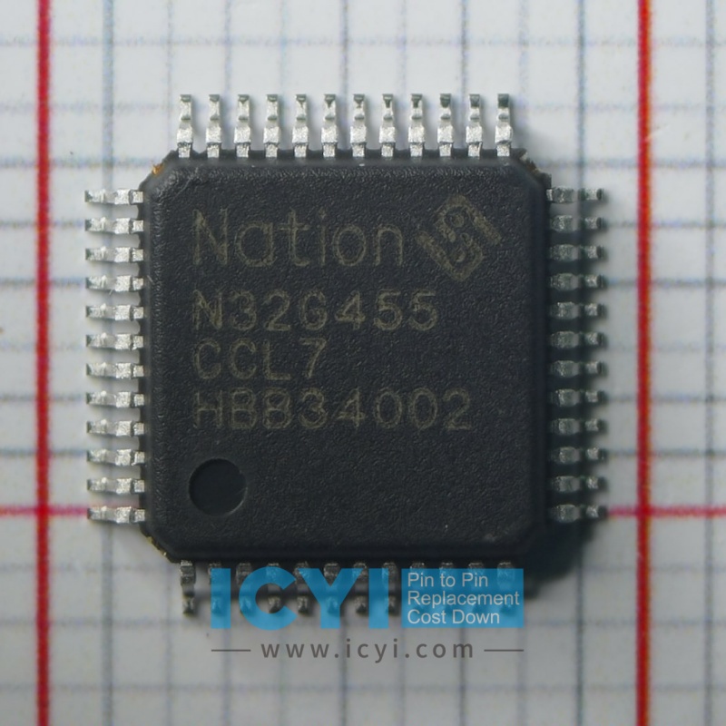
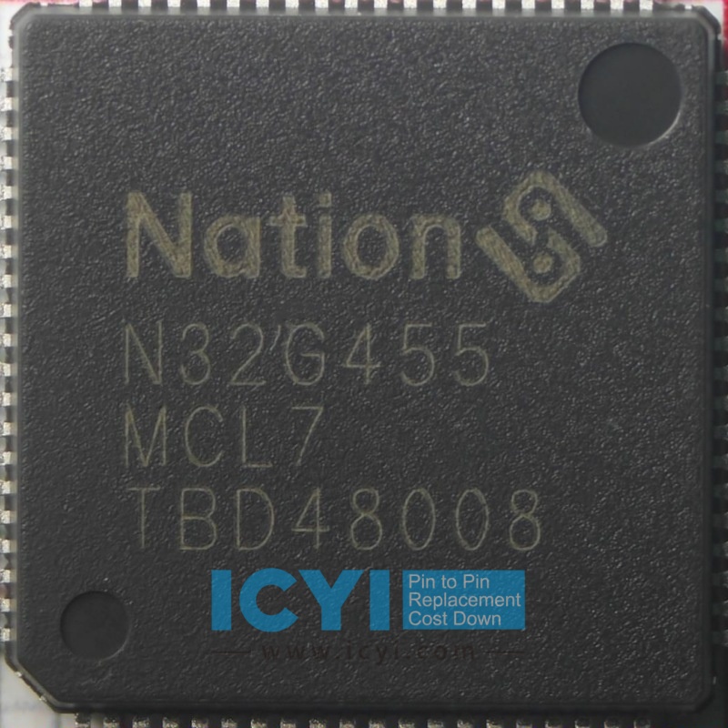
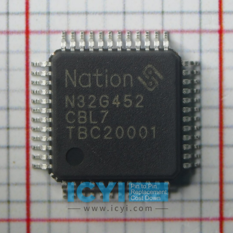
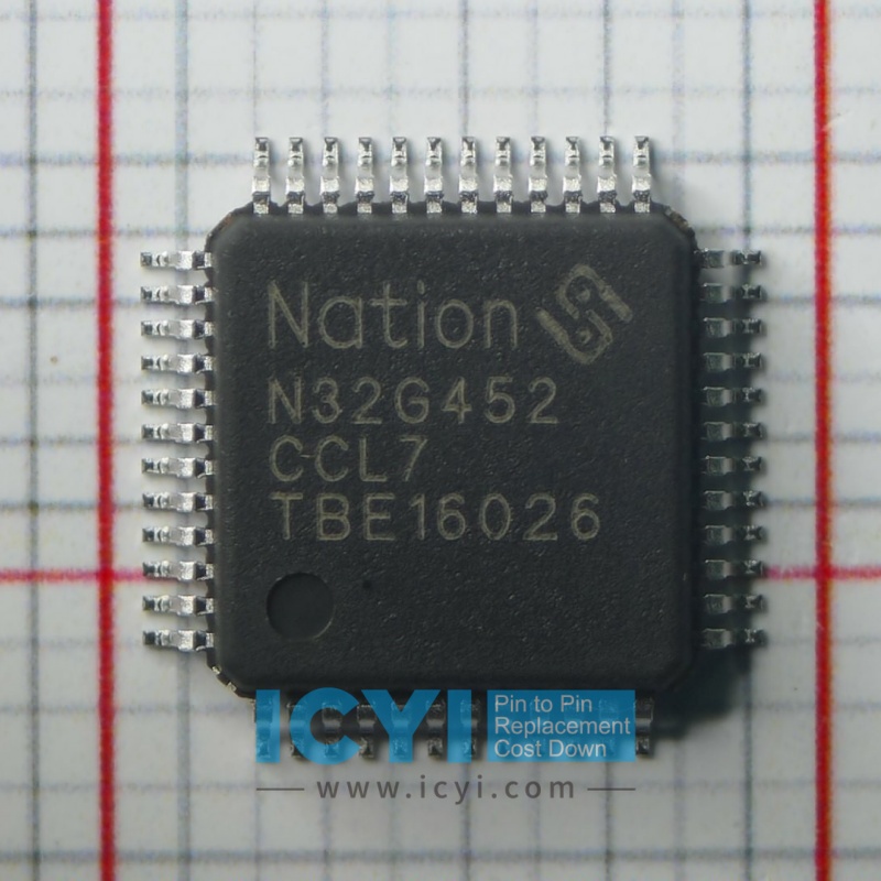
• Package
— QFN48(6mm x 6mm)
— QFN64(8mm x 8mm )
— QFN88(10mm x 10mm)